


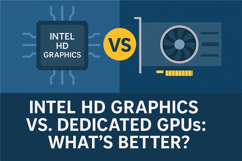


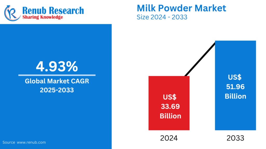


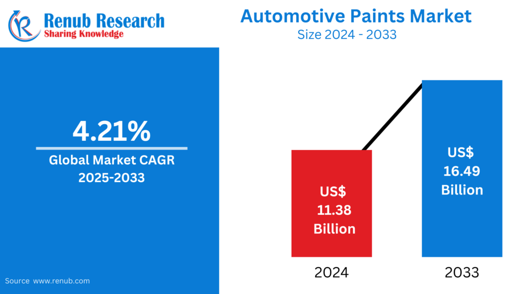


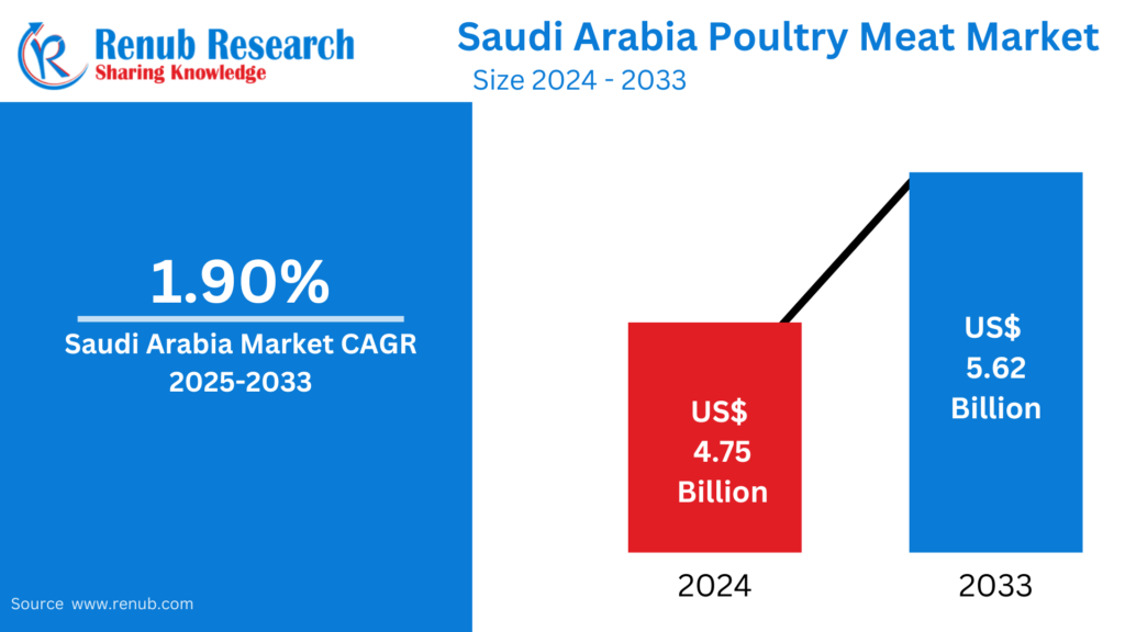


 01
02
01
02
 04
02
04
02
 01
01
 02
02
 03
03
 04
04
 01
02
01
02
03
01
02
01
02
03
 04
01
02
03
04
01
02
01
02
03
04
01
02
03
04
04
01
02
03
04
01
02
01
02
03
04
01
02
03
04
 01
02
03
04
02
03
04
01
02
03
04
02
03
04
 01
02
03
04
01
02
03
01
02
03
04
01
02
03
 04
04
 05
06
01
02
03
04
05
05
06
01
02
03
04
05
 06
01
02
03
04
05
06
06
01
02
03
04
05
06


 01
02
01
02


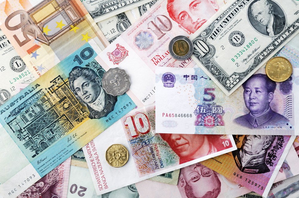
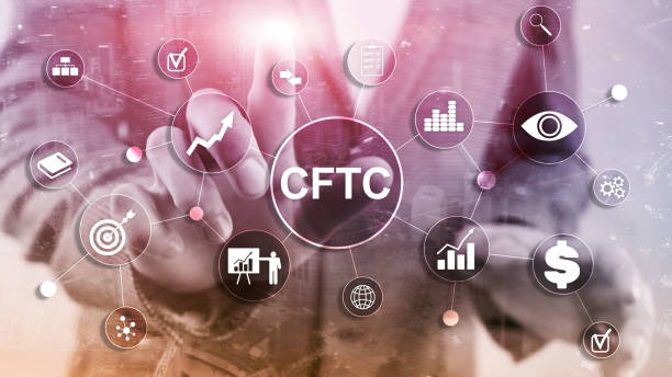
In today’s fast-paced financial world, having the right investment knowledge can make all the difference. Many individuals in India are
No labor certification is required. No job offer or permanent position is needed. Self-petition is allowed. The EB-1A immigrant visas
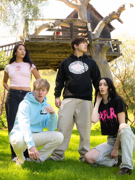
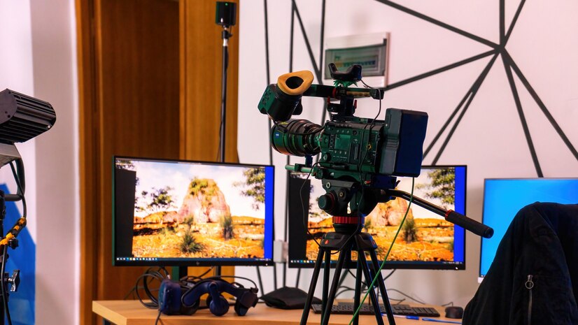
In 2025, TikTok continues to dominate social media, with millions of videos being uploaded and shared every day. From viral
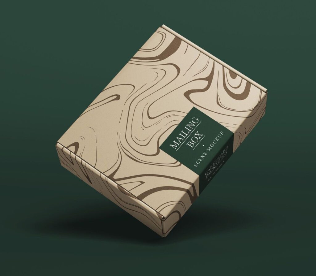
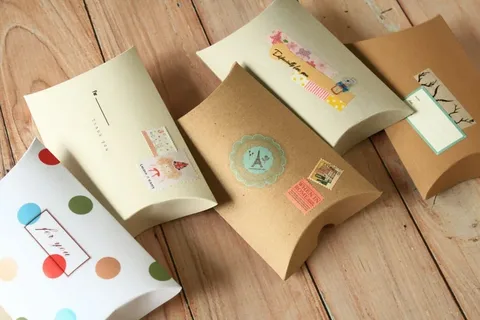
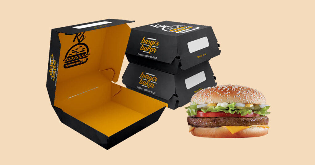
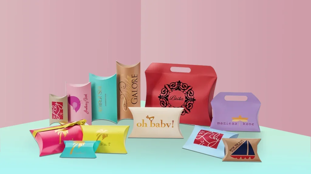
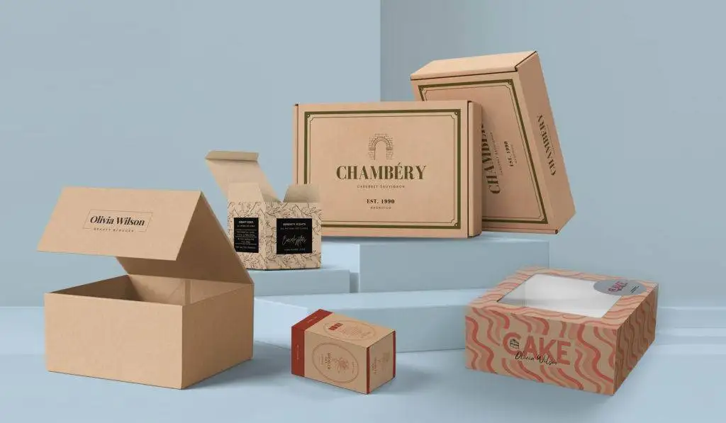
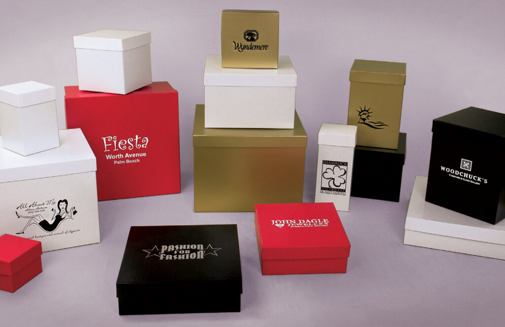
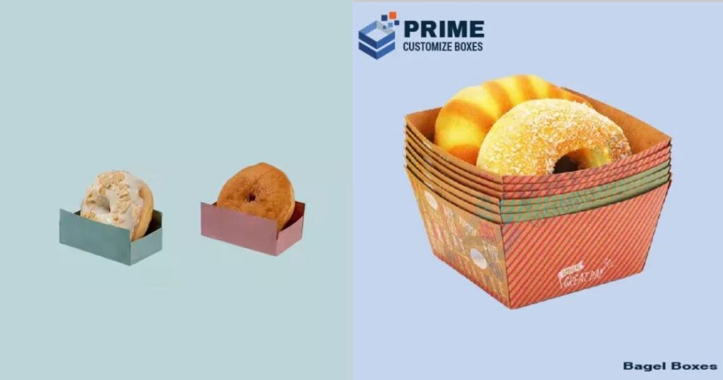
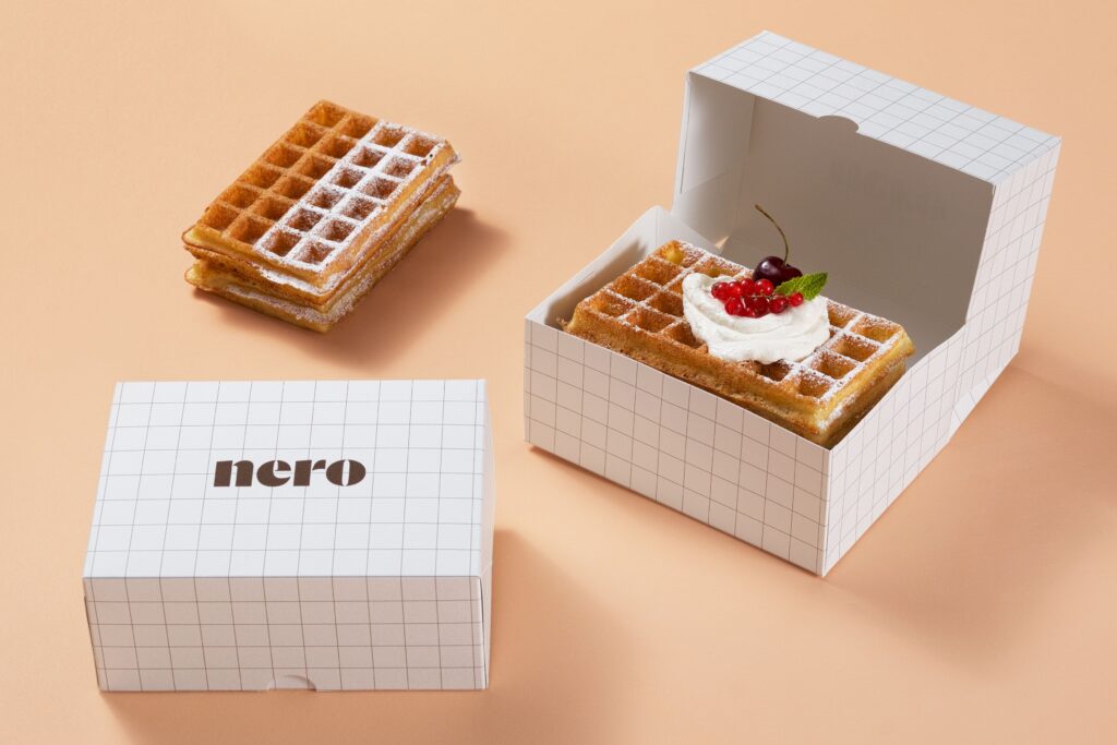
Frozen pizza that comes in custom frozen pizza boxes is important in ensuring the protection of the frozen goods during
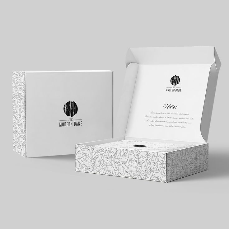
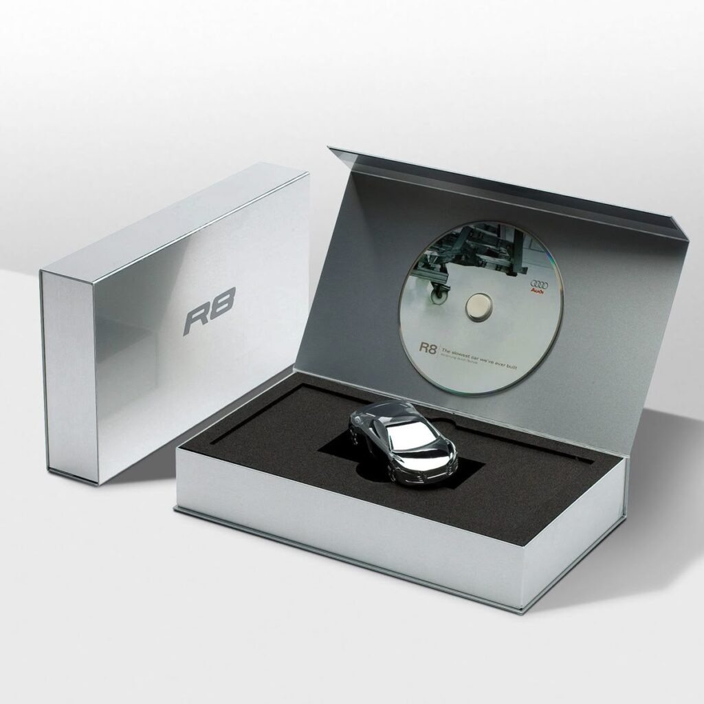
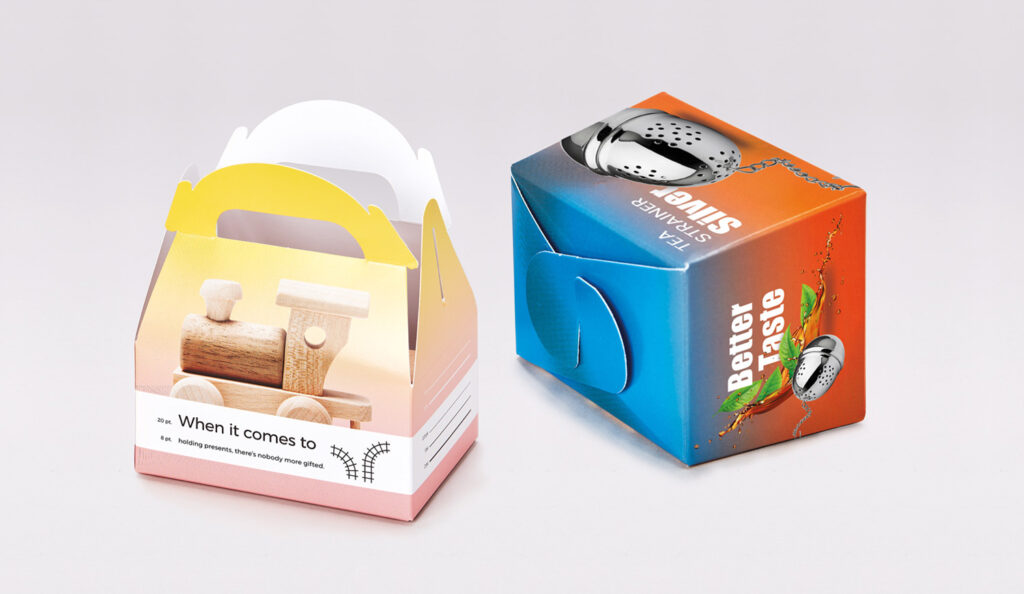
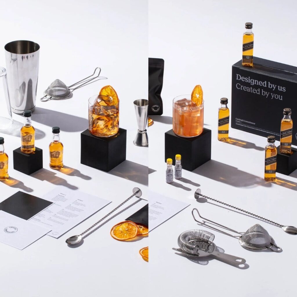
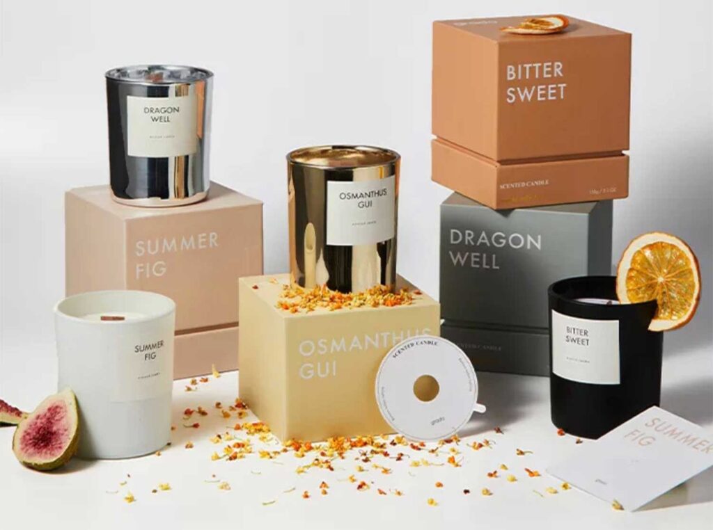
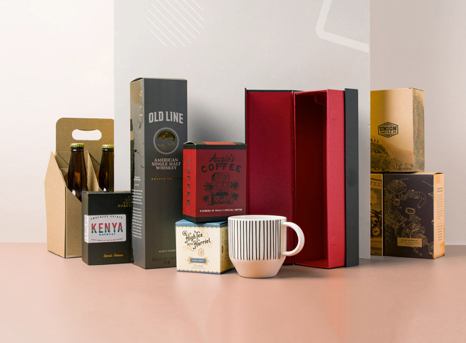
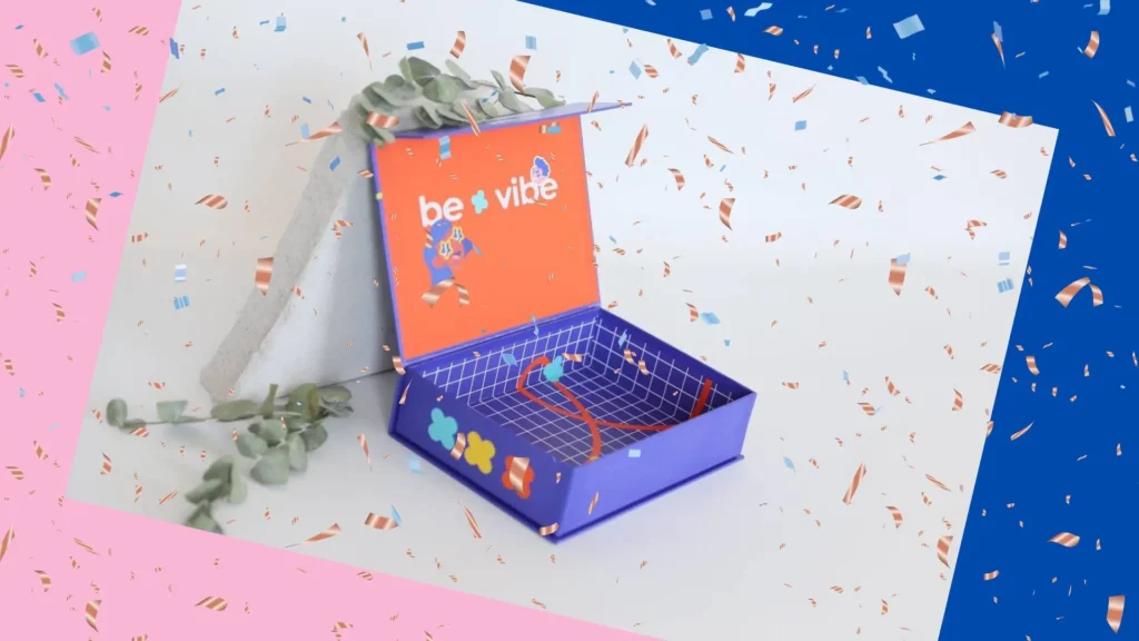
Custom subscription boxes are a commonplace in the rapidly changing environment of the e-commerce world and provide consumers with an
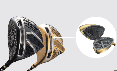
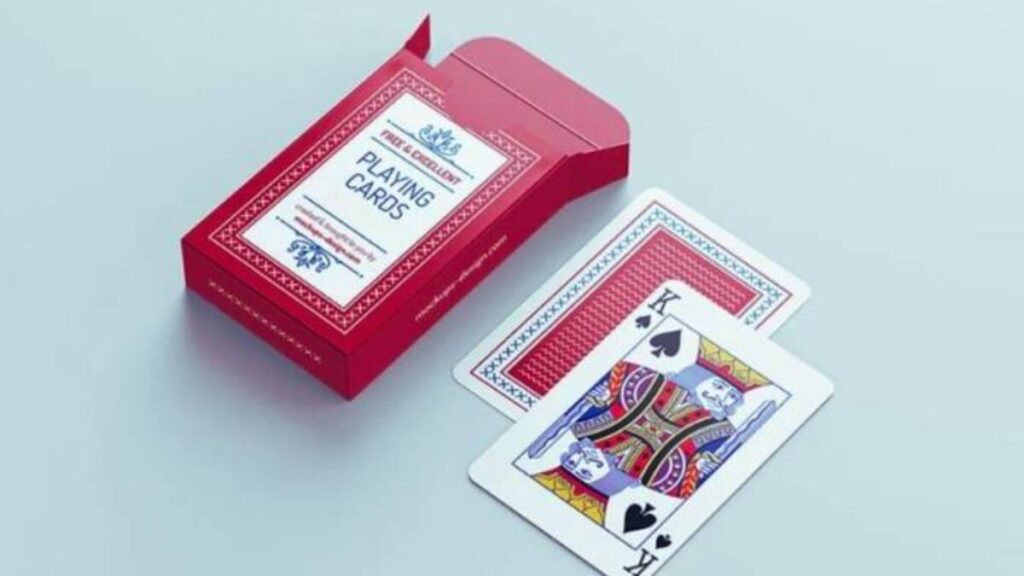
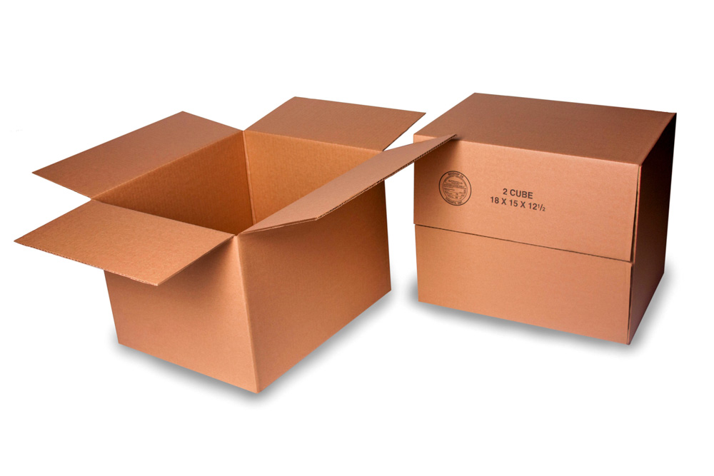
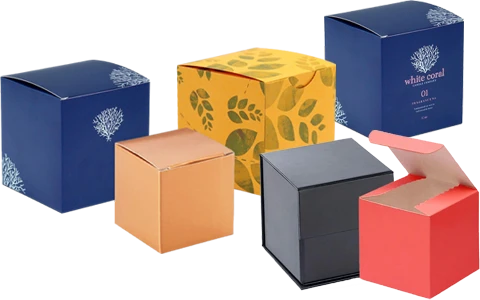
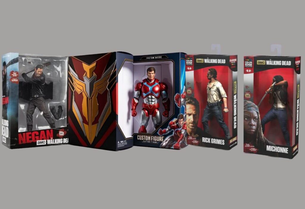
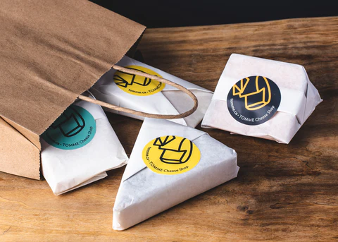
Custom die cut boxes Canada are the most precise, durable, and tailored to the businesses that want to have unique
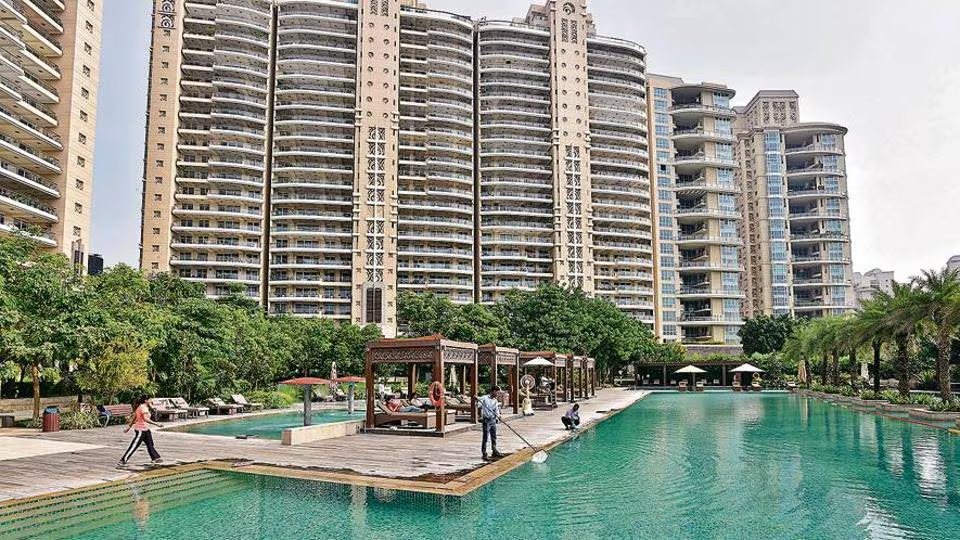
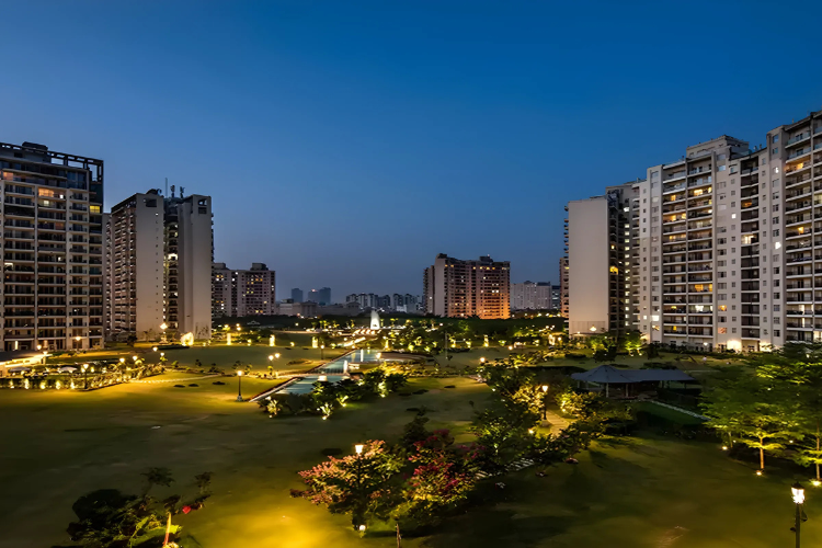
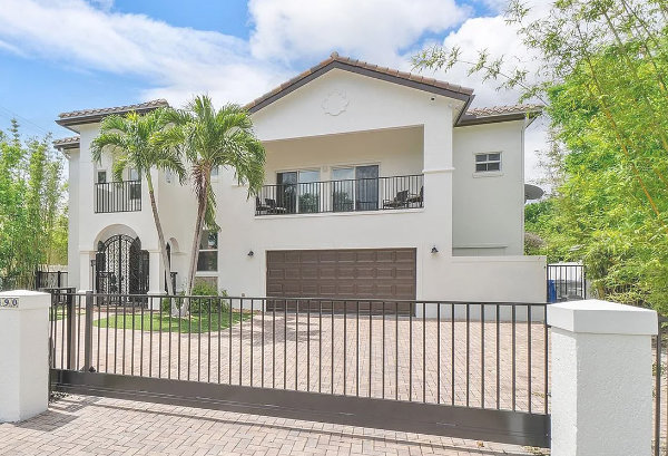
Jerusalem, a city where ancient heritage meets modern sophistication, offers a truly unique real estate landscape. Whether you’re drawn to
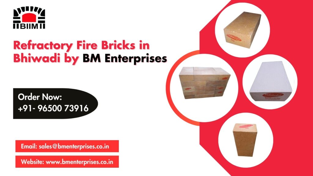
When it comes to fire safety, prevention and preparedness are non-negotiable. Whether you’re running a construction site, hosting an event,
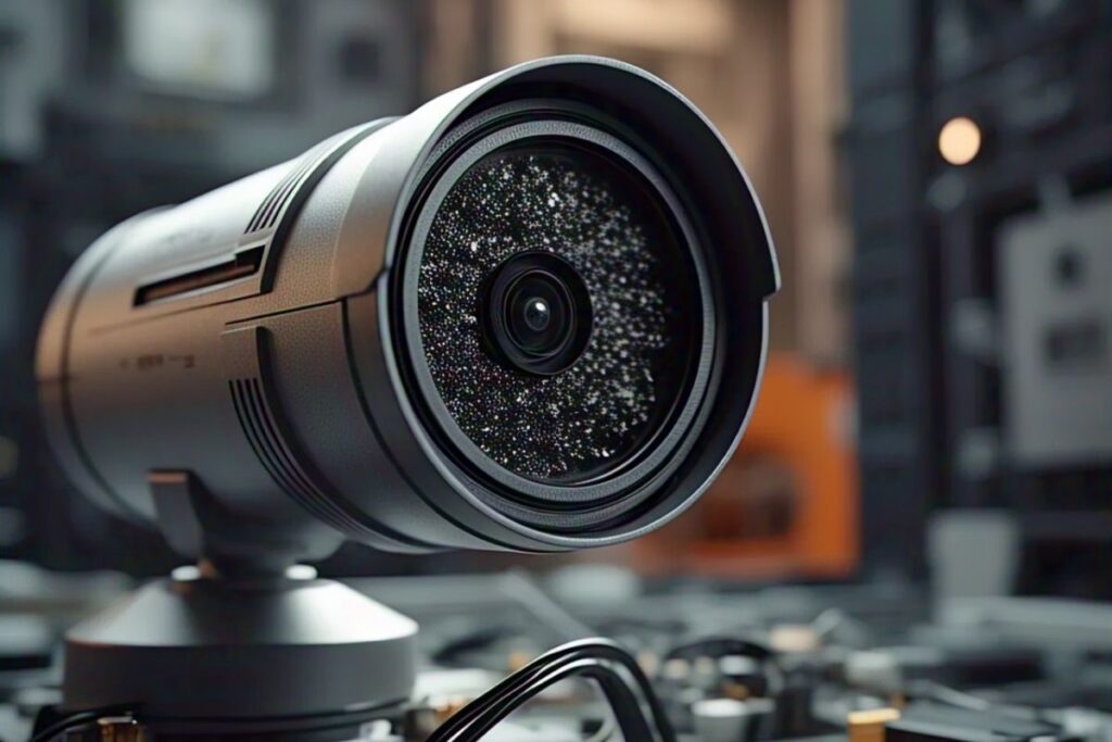
Security is no longer just an optional service for businesses and property owners in Los Angeles. Rising crime rates, busy
The fast-paced world of digital is a race for visibility, leads, and credibility for businesses both large and small. Most
In today’s fast-paced digital world, downloading MP3s from YouTube has become incredibly popular. Millions of users rely on online tools
Downloading YouTube videos has become a common habit for users who love downloading their favorite music, tutorials, and entertainment content
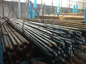
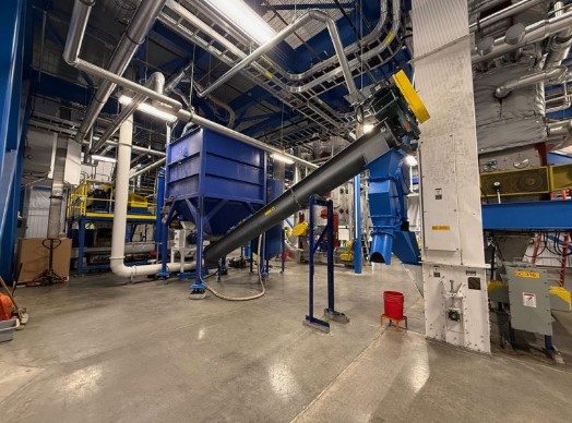
For decades, Chennai has been regarded as one of India’s most vibrant manufacturing and industrial centers. Home to major automakers, logistics firms, and exporting houses, the city’s need for strong, inexpensive, and effective packing supplies has grown dramatically. Packaging has
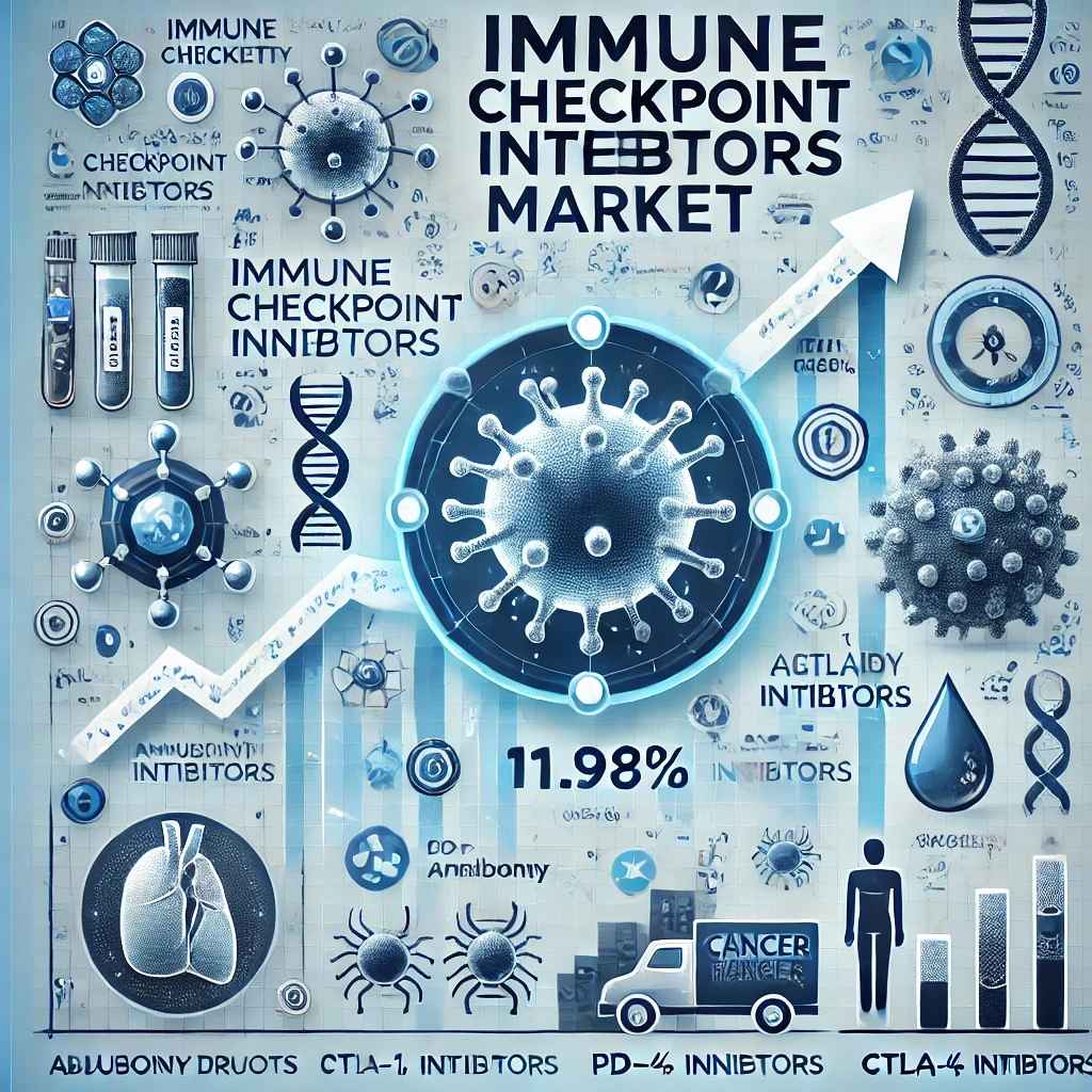
India’s biotechnology sector is witnessing a transformative shift, powered by innovation, global partnerships, and the demand for advanced life sciences
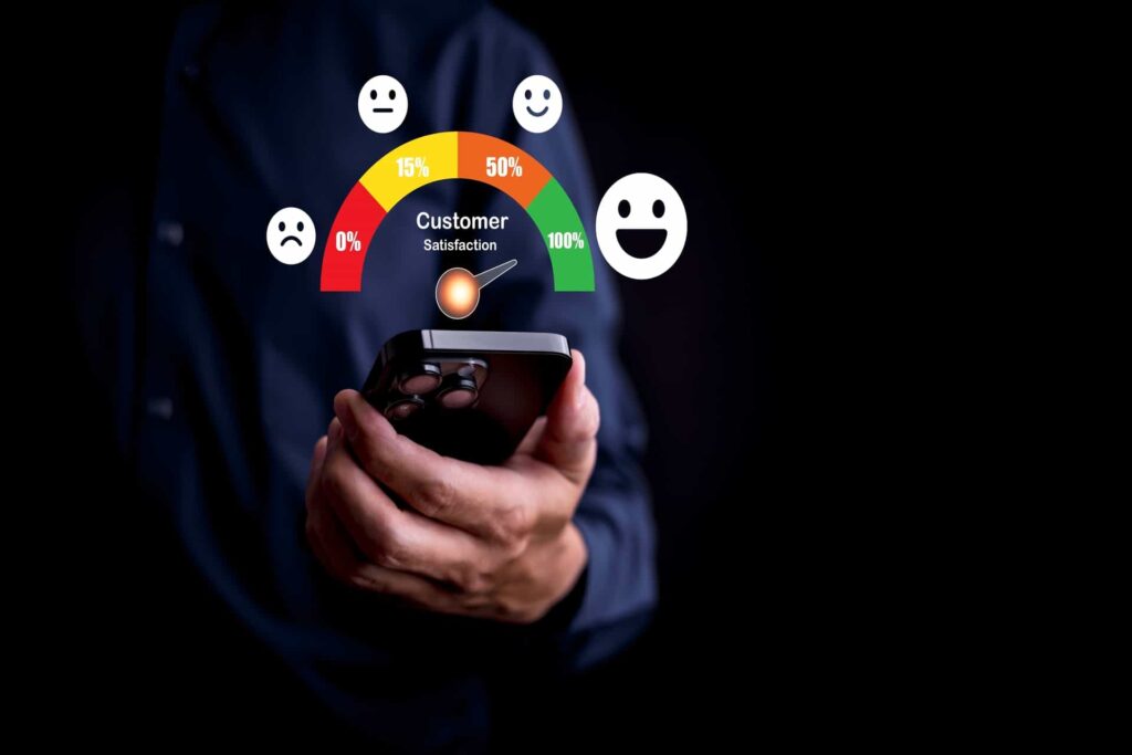
Tone down chasing shiny new leads. Your biggest chance for growth is already right there, sitting in your customer list.


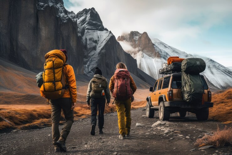
This may be the latest case of post aggression emigration in Ukraine. But it is unlikely to be the final stage for millions of people to leave the country. These people do not want
 English